Process Wastewater Treatment System
BIM / Revit Modelling for the Semiconductor Industry
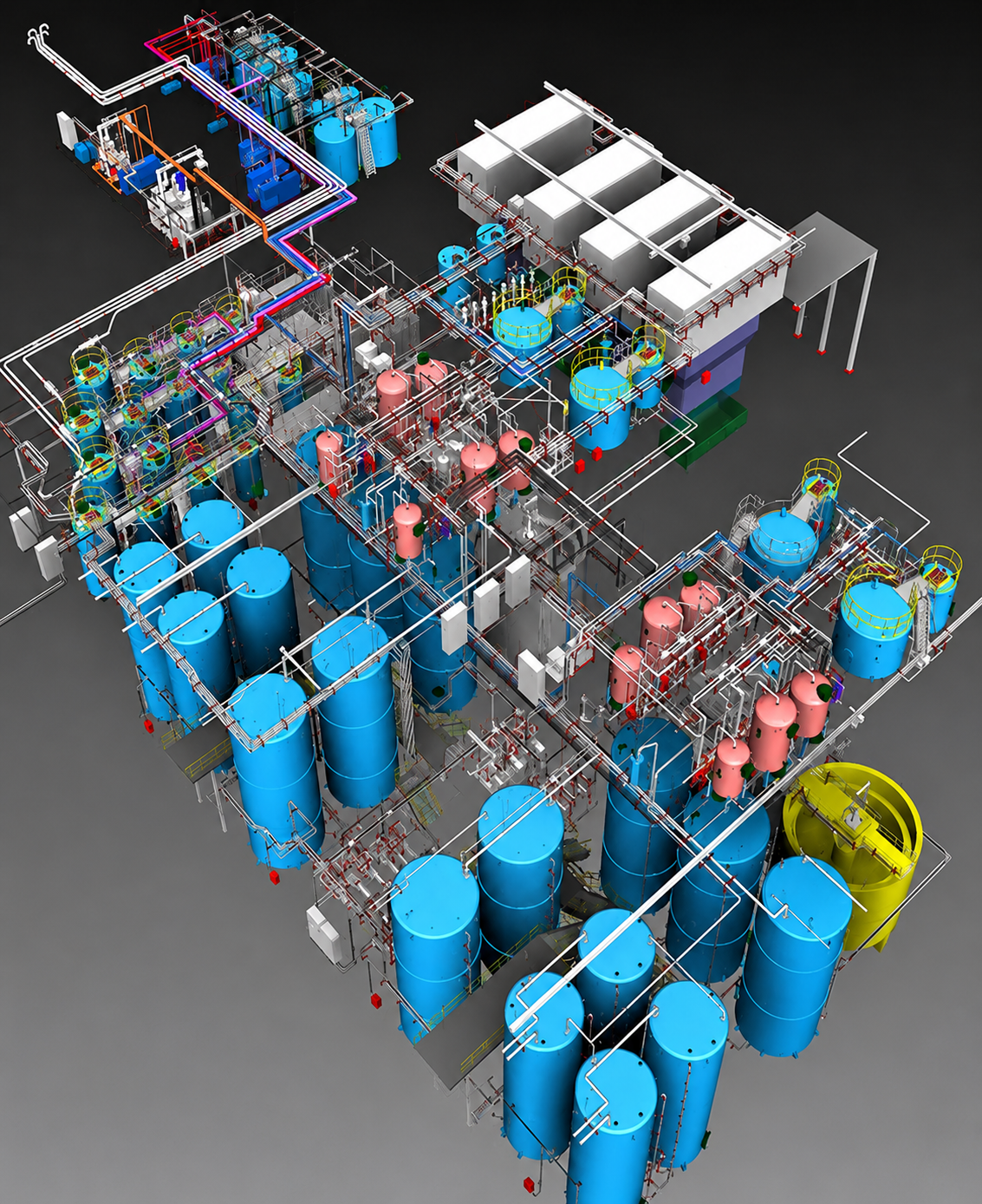
Overview
Semiconductor manufacturing places some of the most demanding requirements on process infrastructure of any industry — tight spatial tolerances, high-purity system integrity, and zero tolerance for design conflicts that could disrupt production. For this project, United Service Consultants is delivering a fully coordinated BIM model of a process wastewater treatment system, engineered to integrate seamlessly with the facility's structural, architectural, and MEP systems from design through construction.
Our approach combines detailed 3D modelling with rigorous multi-discipline coordination, ensuring the process piping design is resolved digitally — long before it reaches the site — where the cost and complexity of correcting a conflict are far higher.
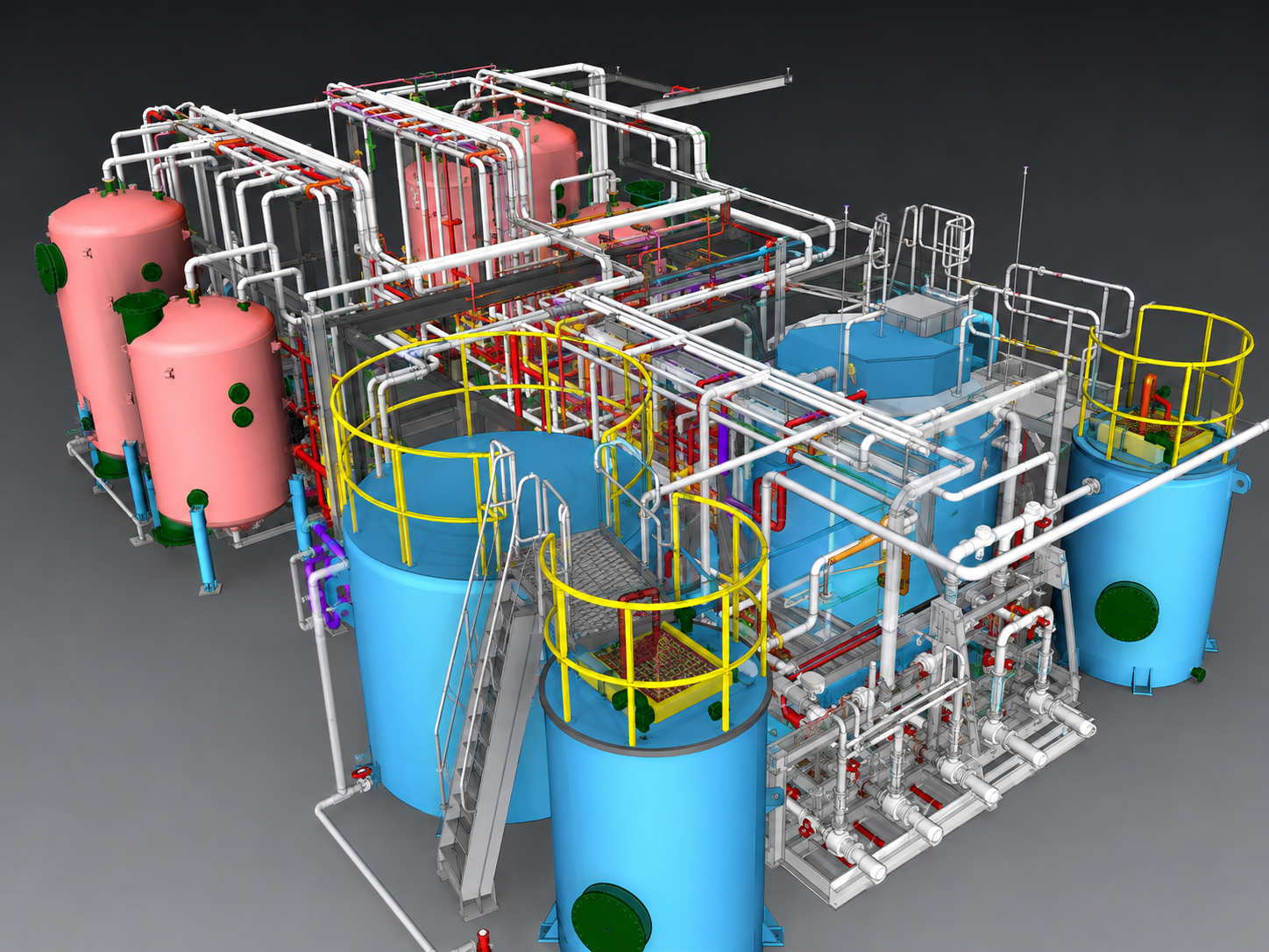
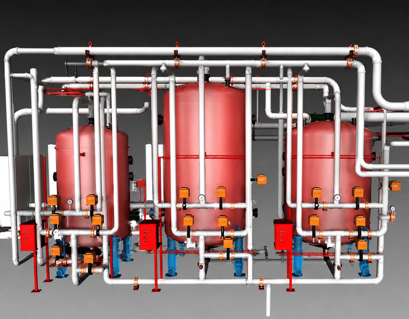
Scope of Work
LOD 350 BIM Modelling
The process piping system is modelled to a level of detail defining precise size, shape, location, and orientation of every component, along with its physical relationship to surrounding building systems — the standard required for construction-ready coordination.
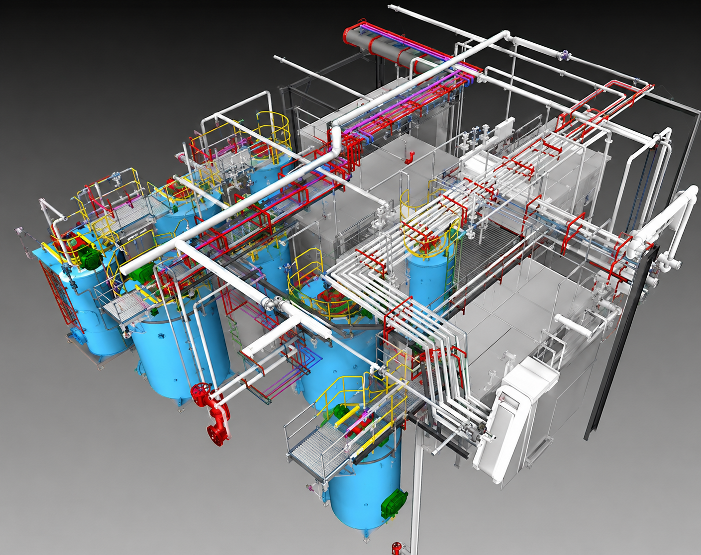
Multi-Discipline Clash Coordination
The process model is cross-checked against structural, architectural, and MEP systems to identify and resolve spatial conflicts before construction begins, protecting project timelines and reducing on-site rework.
Interested in a similar project?
Contact Us